看了太赫茲近場光學顯微鏡- THz-NeaSNOM的用戶又看了
 留言詢價
留言詢價
虛擬號將在 180 秒后失效
使用微信掃碼撥號
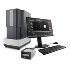
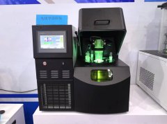
太赫茲近場光學顯微鏡 - THz-NeaSNOM
--30nm光學信號空間分辨率
太赫茲(THz)光源波長較大,一般在300微米左右。由于衍射極限的存在,THz遠場測量系統的光學空間分辨率一般被限制在150微米左右。該THz光遠場測量結果的準確度經常無法滿足對材料科學研究,尤其是需要納米分辨率的微細尺度材料分布研究(例如半導體芯片中各個組成:源極,漏極,柵極)的實驗。THz-NeaSNOM近場光學顯微鏡的出現為此難題提供了一個很好的解決方案。
德國neaspec公司與Fraunhofer IPM在neaspec公司neaSNOM近場光學顯微鏡的基礎上,已經成功研發了一套易用使用且THz系統的空間分辨率達到30nm的實驗設備。
產品特點/基本參數
+ 優于30nm的空間分辨率 + 常用THz光范圍:0.1-3THz + **設計的寬波段拋面鏡 + THz研究可使用商業化的AFM探針 + THz-TDS使用飛秒激光光源 + 簡單易用,穩定性高 |
半導體結構表征—30nm空間分辨率
THz-NeaSNOM近場光學顯微鏡(下圖左)對半導體結構的測量結果圖。
該結果表明硅襯底(上圖左,灰色)上的SiO(一氧化硅)的尺寸大約在1.5×1 平方微米。通過分析左側的高度數據,可以知道該一氧化硅結構僅僅只有大約22納米厚度。雖然該層狀結構非常薄,但THz-NeaSNOM近場光學顯微鏡(下圖左)在測量高度的同時仍然能夠記錄該結構與襯底的近場光學信號的明顯不同襯度的結果。該THz-NeaSNOM近場光學顯微鏡不僅在測量非常薄樣品的時 候靈敏度非常高,而且通過分析近場光學信號數據(下圖右)也證實了它超高的空間分辨率(~25-30nm)。
表征半導體器件 Nature 456,454(2008)
超快機制研究納米線 Nature Photonics 8,841(2014)
部分用戶好評與列表(排名不分先后)
neaspec公司產品以其穩定的性能、極高的空間分辨率和良好的用戶體驗,得到了國內外眾多科學家的認可和肯定......
"The neaSNOM microscope with it’s imaging and nano-FTIR mode is the most useful research instrument in years, bringing genuinely new insights." Prof. Dmitri Basov 美國 加州大學 University of California San Diego Department of Physics La Jolla, USA | |
"We were looking for a flexible research tool capable of characterizing our energy storage materials at the nanoscale. neaSNOM proofed to be the system with the highest spatial resolution in infrared imaging and spectroscopy and brings us substantial new insights for our research” Dr. Jaroslaw Syzdek 美國 勞倫斯伯克利國家實驗室 Lawrence Berkeley National Laboratory Environmental Energy Technologies Division Berkeley, USA | |
"The neaSNOM microscope boosted my research in plasmonic properties of noble metal nanocrystals, optical resonances of dielectric nanostructures, and plasmon polaritons of graphene-like two dimensional nanomaterials." 陳煥君 教授 中國 中山大學 Sun Yat-sen University China | |
"As a near-field expert I was quickly convinced that neaSNOM is the only optical AFM microscope completely satisfying the needs of demanding near-field experiments. It’s the best comercially available technology and in addition really easy to use." Prof. Thomas Taubner 德國 亞琛工業大學 RWTH Aachen Metamaterials & Nano-Optics Aachen, Germany | |
"As a newcomer to the near-field optics I am very grateful for the prompt and competent support provided by neaspec’s experts." Dr. Edward Yoxall 英國 帝國理工大學 Imperial College London Department of Physics London, United Kingdom | |
"After many years of research and development in near-field microscopy, we finally made our dream come true to perform infrared imaging & spectroscopy at the nanoscale. With neaSNOM we can additionally realize Raman, fluorescence and non-linear nano-spectroscopy." Prof. Rainer Hillenbrand 西班牙 納米科學協同研究中心 CIC nanoGUNE Research Center Co-Founder and Scientific Advisor San Sebastian, Spain | |
"A unique advantage of the neaSNOM microscope is that it can be applied to many fields of scientific research such as Chemistry, Semiconductor Technology, Polymer Science and even Life-Science." Dr. Fritz Keilmann 德國 慕尼黑大學 Ludwig-Maximilians Universit?t München Co-Founder and Scientific-Advisor Munich, Germany |
南京大學 | 中山大學 |
首都師范大學 | 蘇州大學 |
University of San Diego,USA | University of Southampton, UK |
CIC nanoGUNE San Sebastion, Spain | LBNL Berkeley, USA |
Fraunhofer Institut ILT Aachen, Germany | Max-Planck-Institut of Quantum Optics, Garching, Germany |
University of Bristol, UK | RWTH Aachen, Germany |
California State University Long Beach, USA…… | |
暫無數據!
 太赫茲近場光學顯微鏡- THz-NeaSNOM的工作原理介紹?太赫茲近場光學顯微鏡- THz-NeaSNOM的使用方法?太赫茲近場光學顯微鏡- THz-NeaSNOM多少錢一臺?太赫茲近場光學顯微鏡- THz-NeaSNOM使用的注意事項太赫茲近場光學顯微鏡- THz-NeaSNOM的說明書有嗎?太赫茲近場光學顯微鏡- THz-NeaSNOM的操作規程有嗎?太赫茲近場光學顯微鏡- THz-NeaSNOM的報價含票含運費嗎?太赫茲近場光學顯微鏡- THz-NeaSNOM有現貨嗎?太赫茲近場光學顯微鏡- THz-NeaSNOM包安裝嗎?


 手機版:
手機版: